Table of Contents
- Hmm...
- The story so far
- To make your own springboard device...
- A minimal SD interface
- Interfacing to the 68k bus
- Drivers
- Finally
- Comments...
Hmm...
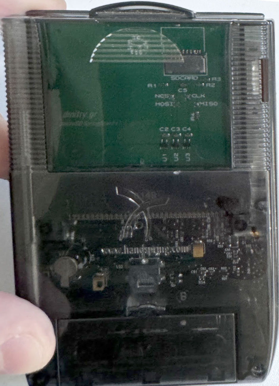
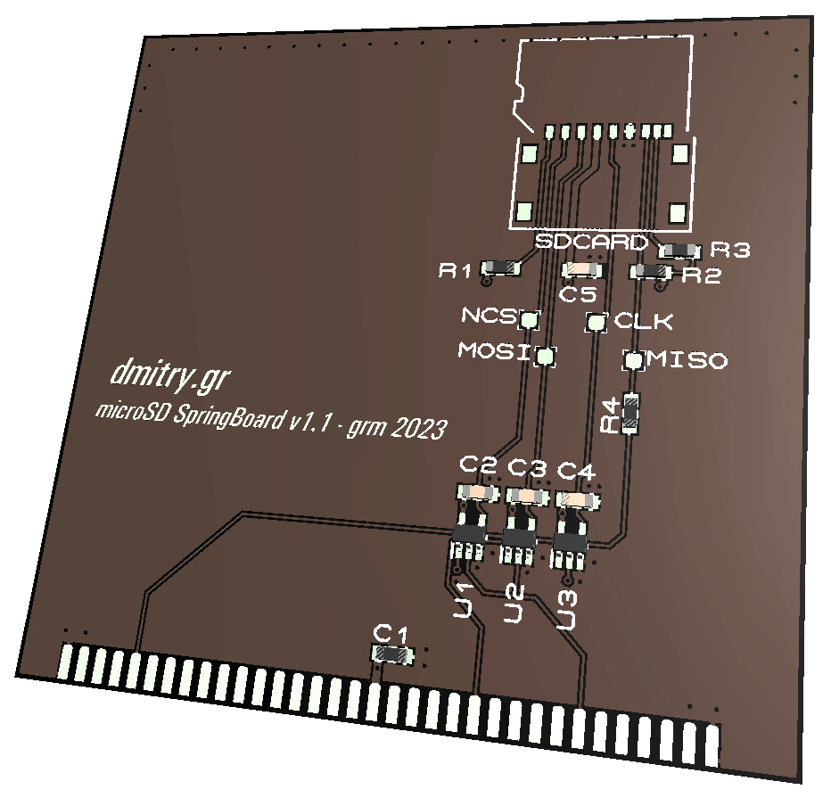
What is the minimal-part-count way to connect an SD card to a Handspring device? Three SOT-23 chips, as you can see in the image. Basically, an SD card wired directly to the 68k bus :)
The story so far
When Handspring released the Visor PDA line, the main distinguishing characteristic of it was the Springboard slot. It was an expansion mechanism via which the device could access wireless internet, make phone calls, play MP3s or radio, capture images, or export the displayed screen image to an external monitor. The springboard slot was very versatile and many accessories for it were made. Its power came from the fact that it was basically a direct connection to the main CPU's bus. The 68k CPU used in the Visor line was the MC68EZ328 for the first few devices. Later devices switched to MC68VZ328. For all practical purposes this is just the SoC version of the good[[citation needed]] old 68k.
Springboard Accessories
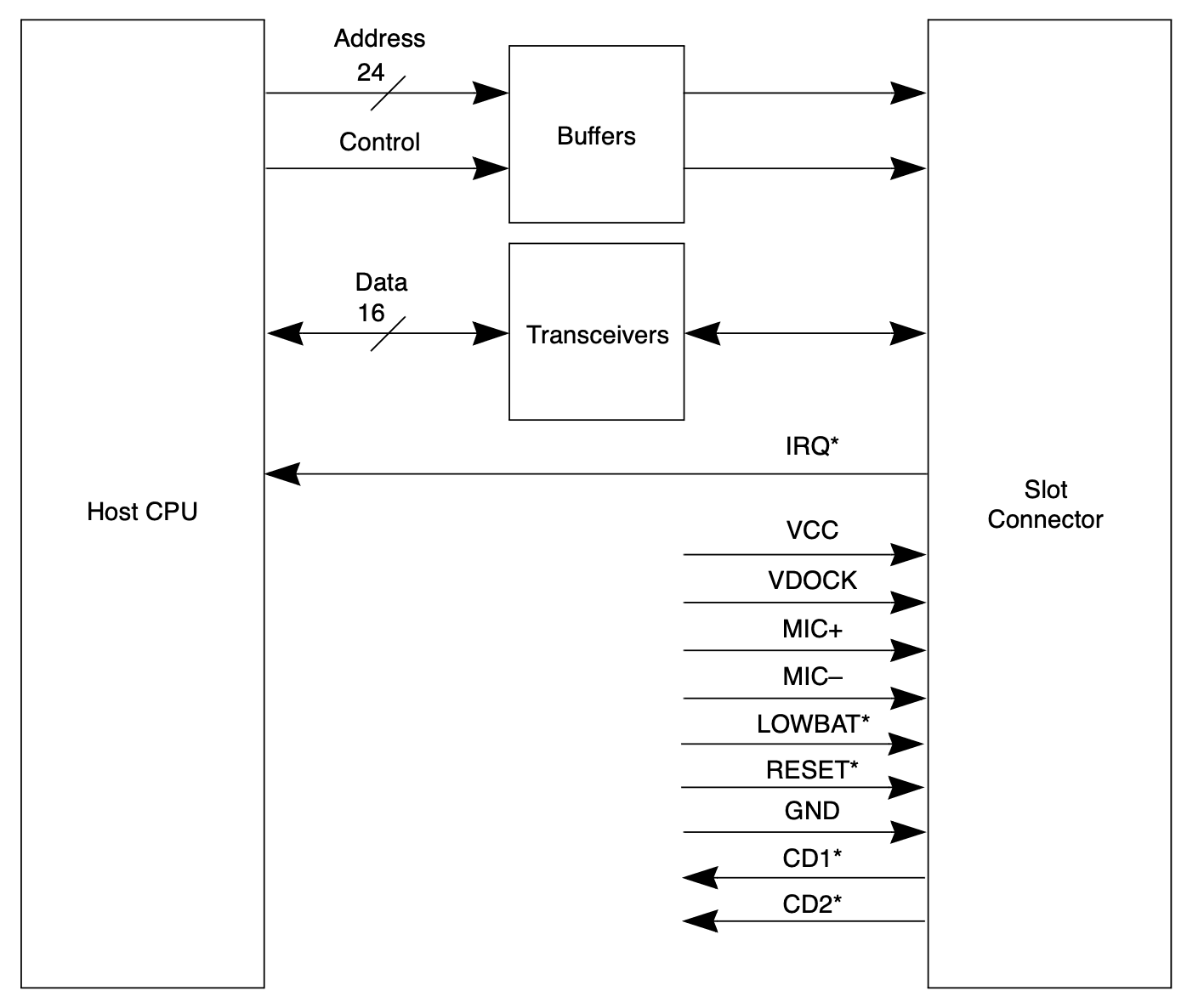
The springboard slot exposes 24 address lines (of which the bottom is never used), 16 data lines, an interrupt request line to the host CPU, two chip select lines, the usual bus control lines (nOE and nWE), and a few other misc things, like power supply, low battery indication, ground, etc. As per the official docs, the bus is always 16-bits-wide (this can actually be configured otherwise, but not via the official API). To the host CPU the springboard device's first chip select is required to look like a x16 ROM containing a valid PalmOS Card. This will usually contain the applications and drivers needed to make use of the module. Some modules only contained software and thus were made of only a single x16 flash chip. The more interesting modules contained some other hardware, and thus used the second chip select to communicate with it.
To make your own springboard device...
The proper way
Handspring published great many documents on how to make proper a springboard device. These contain all the info one needs to create a proper springboard-compatible accessory. The main issue you'd face today is the 34x2 1.27mm connector. It is similar to PCMCIA, but with different plastic keys around it. The other option is to use a connector without keys. There are such connectors available in some places, but they are becoming more and more rare. I found a source of them on LCSC and ordered a few dozen for all my future projects.
The second required part is the ROM to contain the driver. It is required officially, but not checked for by the device.
The cheapskate way
If you are willing to be a bit of a pain for the users, however, you can skip the ROM and tell them to load the driver in another way (infra-red or pc-sync). This would violate the requirements and your module would not be approved by Handspring. Handspring no longer exists, so we can live with that. Not having the ROM onboard allows for a much simpler board and fewer parts. A win!
A minimal SD interface
SPI
The SD protocol provides for a simple way to communicate with an SD card - SPI. This has been supported since long before dinosaurs roamed the earth, and there are rumors that even single-celled organisms at the dawn of time interfaced to the SD cards of yore via SPI. The SPI protocol requires four unidirectional lines. The first is nCS is used to select the card and tell it that upcoming communication is with it. It is normally high, and must go low for every transaction with the SD card. The second is CLK and is the clock for the interface. SD card protocol over SPI is explicitly byte-based (SDIO protocol is not) and so clock pulses will always come in groups of eight. The last two are MOSI and MISO. These are the data lines that, when indicated by the clock pulses, carry the data to and from the card.
There are a few things about SPI that we can make use of. First is that a proper SPI slave does not care about what the MISO, MOSI, and CLK lines do while the nCS line is high. In real SPI systems this is what access to other slaves would look like. In theory, in SPI mode 0 (the only one that matters), no device should care what MOSI does while the clock line is not changing. That should give us more leeway about what we do with the MOSI line.
Interfacing to the 68k bus
The first congruency
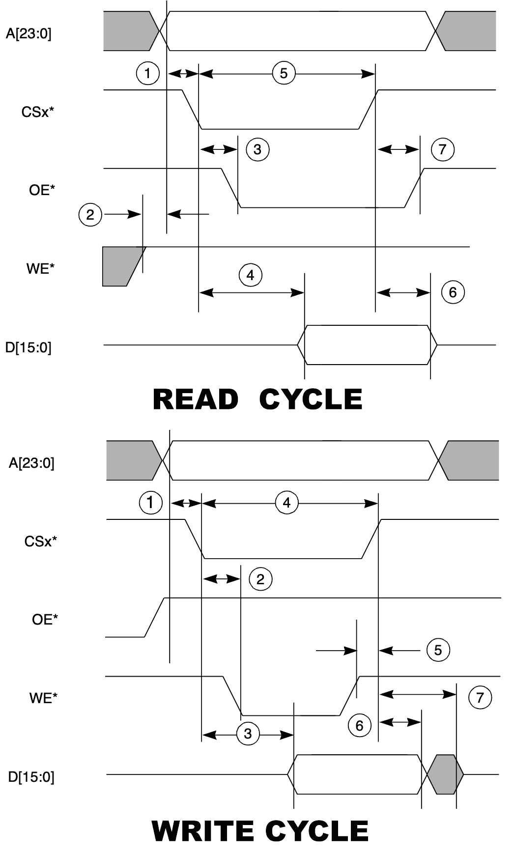
Handspring docs (as well as the MC68k docs) explain the 68k bus cycles quite well. Here you can see both the read and the write cycles. It looks nothing like SPI. Not even a little. So what can we do? First, let's look only at read cycles. Imagine the chip select line being inverted. Suddenly you see that you can consider any address line to be MOSI, any data line to be MISO, and the inverted chip select as CLK. This is something we can build on.
Chip select
Clearly there is no signal that we can control long term to act as nCS for the card. We'll need something that can hold a state until changed somehow. That's a D-latch. We can use the other chip select to trigger it, and any address line as the data input. Thus, a read access to the proper address can be used to set and reset its output. I chose 74LVC1G80GW for this, as it is easily available in a cute SOT-23 package. (The inverter I used is also a SOT-23 - the 74HCT1G04GW). With this we seemingly have all the building blocks we need and we're only using two tiny chips. All done, right?
Not so easy
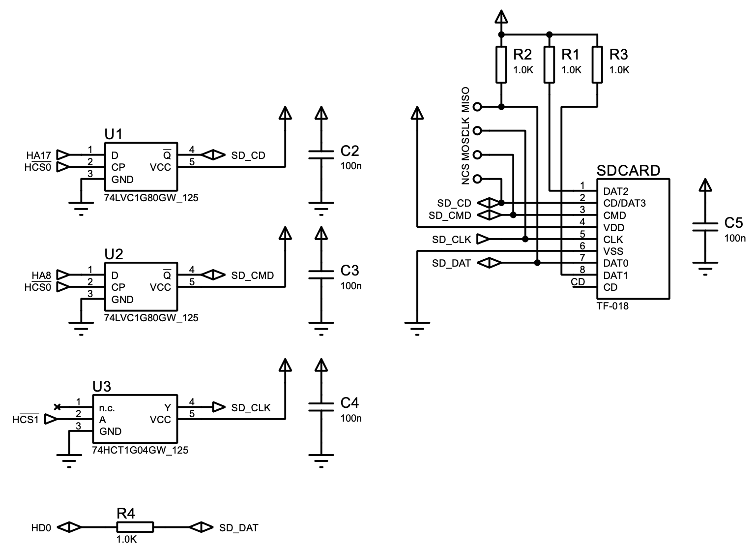
I tried this design and it did not work. The issue is that our MOSI line will move wildly while CLK is stable, since we're seeing all the 68k bus accesses. Now, in theory, this should not matter, but in practice all the SD cards seem to care. So what can we do? Stick another latch into there, of course. And...that works... Here you can see the final schematic.
So what are the bus accesses needed? As I had mentioned, only read accesses are used, since we use data pins for output and address lines for input. Bit 17 of any access (inverted) becomes the new value for card's nCS pin. Bit 8 (inverted) becomes the MOSI that the card sees. This means that doing a read to chip select 1 address 0x20100 will set MOSI low and nCS low. A read access to any address in chip select 2 address space will clock a bit in from the card (on data line 0). Thus, we've sent a 1 to the card and read in a bit. An access to chip select 1's offset 0x20000 will set MOSI high while keeping nCS low. This is how a zero is sent to the card. So, for every SPI bit transacted we need to do two accesses. This is not too bad speed-wise. For pure read transactions (when MOSI state need not change), we can read in a bit in only one access. This is quite fast.
Drivers
The basics
Some Handspring devices shipped with PalmOS old enough that it would not properly support installing Expansion Manager. Luckily I had resolved this problem before. From there, I picked up the PalmOS patches, a FAT12/16/32 filesystem driver, and the patched Expansion Manager. The only thing left was to write a Slot Driver that accesses this hardware properly. I configure the chip selects to be 1MB in size each, starting at 0x28000000, and the rest is as simple as promised:
Polish
The code above is pretty slow. But this is good since SD card init needs to be done at a clock of 400KHz or less. After init is completed, higher clock rates are allowed. This will require assembly. The situation where speed is most important is reading the data, so the most effort went into that. A few clever tricks go into this, including the fact that reading a 32-bit value from a 16-bit interface will perform two back-to-back accesses, much faster than they could be performed any other way. Additionally, MOSI can just stay high the entire time and needs no changes. Here is what the code looks like that will read "sz" bytes into a block pointed to by "data", assuming that size is a multiple of two bytes and data is appropriately aligned.
Why do I need to mask the data with 0x00010001? Because I do not drive the data lines other than 0. This AND instruction could be removed if I were to include 15 pull-down resistors on the card, but that would make it less simple, and I like simple. There is also an assembly implementation of write, but that is less interesting. You can see it in the source code archive.
Finally
So, does it work? Yes, it does and the boards (which George graciously designed in ten minutes) can be assembled for $3 each at JLC. With my driver, any Handspring device with this $3 board can now read/write SD cards, and so can all PalmOS applications. This same cheap SD-card-interfacing method can be used for any other 68k device! All the hardware design files can be downloaded here. The slot driver sources and binaries are here. You'll also need the following files from the SASD page: ExpansionMgr, SlimFat, and RetroFix. The license is simple: free for all non-commercial use. For commercial use (like if you wish to sell kits of this project), contact me.
Comments...
